SEM/FIB
The EPS Focused ion beam (FIB) facility was funded by Scottish Funding Council and set up within the School of Engineering and Physical Sciences at Heriot-Watt University in April 2010. The FIB facility – FEI Quanta 3D FEG is the most versatile high resolution Scanning Electron Microscope (SEM) / FIB for 2D and 3D micro & nanofabrication and material characterization and analysis.
Capabilities
- Novel Field Emission electron optics deliver clear and sharp electron imaging (1.2nm resolution)
- High and low vacuum SEM mode for conductive and non-conductive samples without coating
- Environmental Scanning Electron Microscope (ESEM) mode (1.5 nm resolution)
- High resolution (field emission) ion optics provide high resolution FIB imaging (7 nm resolution)
- High current (1.5pA – 65nA) FIB enables fast material removal (14nm resolution for fabrication)
- Secondary Electron detectors (SED, LV-SED and Gaseous SED) and Low-KV, Solid-State Backscattered Electron Detector (SSBSED) for material characterization
- Three Gas injection System: Platinum deposition, Insulator deposition and Select carbon mill
- Five-axis motorized X-Y-Z-rotate-tilt stage (X=50 mm, Y=50 mm, Z=25 mm, R=360°, T=-15°~75°)
Functions
- High-vacuum SEM (< 6*10-4 Pa): This mode can be used for the examination of vacuum compatible conductive, or gold/carbon coated non-conductive samples.
- Low-vacuum SEM (10 to 130 pa): A low vacuum mode is suitable for the examination of uncoated non-conductive samples such as textiles and papers. Imaging is provided by a Backscattered Detector, giving good elemental contrast details, as well as topographic information. It also allows for secondary election imaging, utilizing the GSE detector. Wet samples can also be examined, but cannot be maintained in a hydrated state.
- Environmental SEM (10 to 4000 pa): A low vacuum mode for the examination of hydrated or gassing samples, where it is desirable to observe the sample in its natural state. Samples are examined uncoated, with a Gaseous SED, within a gaseous environment. It also allows for back scatter imaging in Environmental mode. This is particularly suited to the study of live organisms, textiles and pharmaceutical products. ESEM mode can also be used for collecting secondary electron images of non-conductive samples such as polymers, plastics and ceramics. Samples can be wetted with water (or oil), and a wide range of experiments can be carried out.
- FIB Micro/nanofabrication: A beam of ions generated from liquid gallium (Ga+) ion source is focused onto the sample surface. The Ga+ primary ion beam hits the sample surface and sputters a small amount of material, which leaves the surface as either secondary ions or neutral atoms. Due to the excellent beam positioning accuracy and stable operating conditions, three dimensional structures down to nanometer scale can be obtained by direct writing.
- FIB imaging: The primary Ga+ beam also produces secondary electrons. As the primary beam scans on the sample surface, the signal from the sputtered ions or secondary electrons is collected to form an image.
- Deposition: FIB can also be used to deposit material via ion beam induced deposition. FIB assisted chemical vapour deposition occurs when a gas is introduced to the chamber and allowed to chemically absorb onto the sample.
Applications
In the past few years, the FIB facility has been extensively used in the following areas:
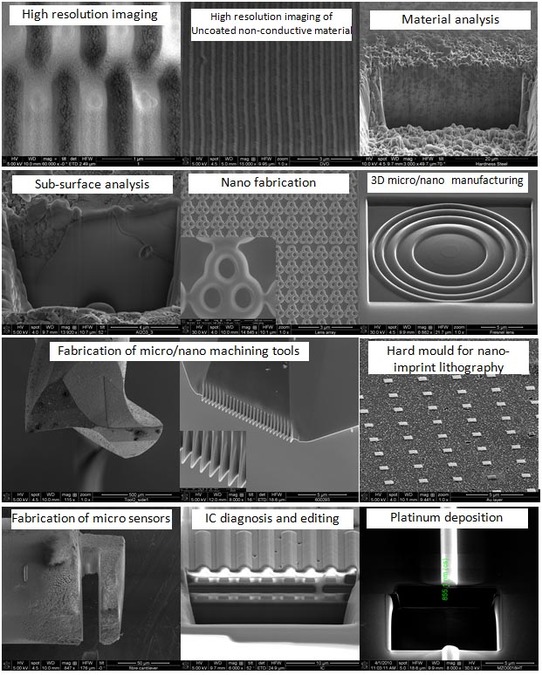
High resolution imaging; High resultion imaging of un-coated non-conductive material; Material analysis; Sub surface analysis; Nano fabrication; 3D micro / nano manufacturing; Fabrication of micro/nano machining tools; hard mould for nano-imprint lithography; Fabrication of micro sensors; IC diagnosis and editing; Platinum deposition.